Please let us in the comment zone any suggestions that you think will improve the article!
If you like the article click the follow button to stay in touch with us!
In this post we will discuss how to generate a sine wave modulated from different PWM signals. These technique it helps us to make pure sine inverters or to generate sine signals with different frequencyes.
As we know(from previous posts) some pins of arduino can generate PWM signals at high frequencies, so we will utilize this and adapt for sine equation. Let’s assume our frequency is 50Hz mean the time period is 20ms. So 10ms is half cycle period. In those 10ms we need to have many pulses with different duty cycles starting with small duty cycles, in the middle of the signal we have maximum duty cycles and finish also with small duty cycles.
To generate a sine wave we will use two pins one for positive half cycle and one for negative half cycle. In our post for this we use pins 5 and 6 that means Timer 0.
For a smooth signal we choose phase correct pwm at a frequency 31372 Hz-see previous post.
One of the biggest problem is that how we calculate the necessary duty cycle for each pulse. So, because our frequency is f=31372Hz the period for each pulse is T=1/31372=31.8 us, so number of pulses for a half cycle is N=10ms/31.8us=314 pulses. Now to calculate the duty cycle for each pulse we have y=sinx, but in this equation wee need degrees so half cycle has 180deg for 314 pulses.
For each pulse we have 180/314=0.57deg/pulse. That means for every pulse we move forward with 0.57deg.
Because it’s unpleasant to calculate each duty cycle by hand below it’s a small program that calculate the duty cycle between 0 and 90 deg( on serial monitor) and between 90 and 180 deg is in the mirror.
The program is:
float x=0;
float y=0;
const float pi=3.14;
int z=0;
float v=0;
int w=0;
void setup() {
Serial.begin(9600);
}
// the loop function runs over and over again forever
void loop() {
if (w==0){
v=x*pi/180; // making deg in radians
y=sin(v); //calculate sine
z=y*250; // calculate duty cycle(250 not 255 because will help to turn off transistors)
delay(100);
x=x+0.57;// increase the angle
}
if (x>90){// we stop to calculate we have the duty cycle for angles smaller than 90deg
// the other half is symetric
x=0;
w==1;
}
Serial.println(z);// on the serial monitor will appear duty cycles between 0 and 90 deg
}
Next we put the values in a vector like:
float sinPWM[]={1,2,5,7,10,12,15,17,19,22,24,27,30,32,34,37,39,42,
44,47,49,52,54,57,59,61,64,66,69,71,73,76,78,80,83,85,88,90,92,94,97,99,
101,103,106,108,110,113,115,117,119,121,124,126,128,130,132,134,136,138,140,142,144,146,
148,150,152,154,156,158,160,162,164,166,168,169,171,173,175,177,178,180,182,184,185,187,188,190,192,193,
195,196,198,199,201,202,204,205,207,208,209,211,212,213,215,216,217,219,220,221,222,223,224,225,226,227,
228,229,230,231,232,233,234,235,236,237,237,238,239,240,240,241,242,242,243,243,244,244,245,245,246,246,
247,247,247,248,248,248,248,249,249,249,249,249,250,250,250,250,249,249,249,249,249,248,
248,248,248,247,247,247,246,246,245,245,244,244,243,243,242,242,241,240,240,239,238,237,237,236,235,234,
233,232,231,230,229,228,227,226,225,224,223,222,221,220,219,217,216,215,213,212,211,209,208,207,205,204,
202,201,199,198,196,195,193,192,190,188,187,185,184,182,180,178,177,175,173,171,169,168,166,164,162,160,
158,156,154,152,150,148,146,144,142,140,138,136,134,132,130,128,126,124,121,119,117,115,113,110,108,106,
103,101,99,97,94,92,90,88,85,83,80,78,76,73,71,69,66,64,61,59,57,54,52,49,47,44,42,39,37,34,32,30,
27,24,22,19,17,15,12,10,7,5,2,1};
First value is 1 because we want to reduce the dead time betwen half cycles of sine signal.
To write the duty cycles we will use OCR0A and OCR0B for timer 0(pins 5 and 6), that means for one half cycle OCR0A will be equal with every component of vector myPWM and for other half cycle OCR0B will do that-see the post with Timer 0.
With the program below we generate phase correct signal at a 31372 Hz and 100 duty cycle(is between 0 and 255 on Timer 0).
void setup() {
pinMode(5, OUTPUT);
pinMode(6,OUTPUT);
TCCR0A=0;//reset the register
TCCR0B=0;//reset tthe register
TCCR0A=0b10100001;// phase correct pwm mode
TCCR0B=0b00000001;// no prescaler
OCR0A=100;//duty cycle
}
void loop() {
// put your main code here, to run repeatedly
}
pinMode(5, OUTPUT);
pinMode(6,OUTPUT);
TCCR0A=0;//reset the register
TCCR0B=0;//reset tthe register
TCCR0A=0b10100001;// phase correct pwm mode
TCCR0B=0b00000001;// no prescaler
OCR0A=100;//duty cycle
}
void loop() {
// put your main code here, to run repeatedly
}
The result is(only for pin 6, pin 5 is exactly like 6):
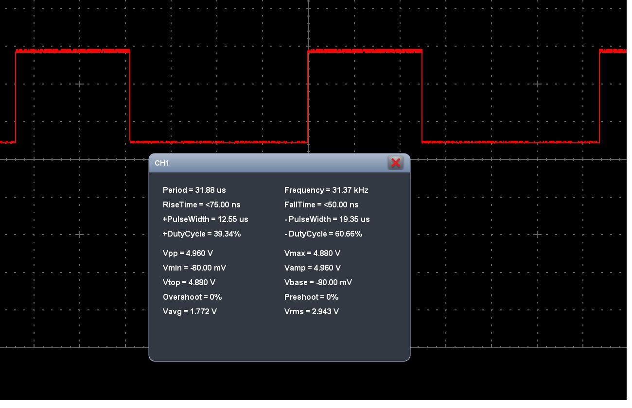
But we want to alternate pins for each half cycle and make a variable duty cycle for each pulse. For this thing we use another timer(Timer 1) in CTC mode with interrupts. We generate a signal with the same frequency as frequency of pins 5 and 6 and after each pulse we change the duty cycle(values from the vector) with an interrupt. At the end of the vector we change pins(half cycle period) and start over.
An interrupt is a part of a program that pause the loop function and execute another part of a program at a very specific time and after that start from where it was.
For this application we use a interrupt that is enabled when Timer 1 match with the OCR1A value. To change the duty cycle at every pulse on pins 5 and 6 we must generate interrupts with a 31372Hz (to enable one interrupt at the same time with an pulse on pins 5 and 6).
To generate that interrupt at every pulse we must set Timer 1 in CTC mode and for that we use TCCR1B register to make WGM12 =1and CS10=1(no prescaling), OC1A must be set in toggle mode in TCCR1A register(COM1A1,COM1A0,COM1B1,COM1B0)see waveform generation mode bit description for Timer 1.
Now we must calculate the value for OCR1A to generate a 31372Hz signal. For that we use the formula from the datasheet with a smal modification, number 2 dissapear fOC1A=fclk/N(1+OCR1A). Explication is that the formula with number 2 is for pwm and to have a frequency to a signal, the signal must be high and low and we wait two counts until compare match, one count before signal became low and one count before signal became high again(picture below). At interrupts when timer hits the compare match value the interrupt is generate, so number 2 dissapear.

The value of OCR1A is determined from OCR1A=(fclk/fOC1A*N)-1 and OCR1A=509.
So Timer 1 start counting until reach OCR1A=509 then activate the interrupt with a frequency 313272Hz.
To enable interrupts we need to set the OCIE1A=1 in TIMSk1 register and use ISR(TIMER1_COMPA_vect) (more details about interrupts here and here).
To be sure there is no problem with interrupts we will use cli() ( stop interrupts) and sei()(enable interrupts).
In ISR function we set the OCR0A and OCR0B with duty cycle values and change this values according to vector, also at the finish of each crossing of vector we change the enabled pin.
Before sine wave we must see if it is everything ok so we have alternate the pins at a stable duty cycle OCR0A and OCR0B equals with 128.
The program for that is below:
int i=0;
int x=0;
int OK=0;
float sinPWM[]={1,2,5,7,10,12,15,17,19,22,24,27,30,32,34,37,39,42,
44,47,49,52,54,57,59,61,64,66,69,71,73,76,78,80,83,85,88,90,92,94,97,99,
101,103,106,108,110,113,115,117,119,121,124,126,128,130,132,134,136,138,140,142,144,146,
148,150,152,154,156,158,160,162,164,166,168,169,171,173,175,177,178,180,182,184,185,187,188,190,192,193,
195,196,198,199,201,202,204,205,207,208,209,211,212,213,215,216,217,219,220,221,222,223,224,225,226,227,
228,229,230,231,232,233,234,235,236,237,237,238,239,240,240,241,242,242,243,243,244,244,245,245,246,246,
247,247,247,248,248,248,248,249,249,249,249,249,255,255,255,255,249,249,249,249,249,248,
248,248,248,247,247,247,246,246,245,245,244,244,243,243,242,242,241,240,240,239,238,237,237,236,235,234,
233,232,231,230,229,228,227,226,225,224,223,222,221,220,219,217,216,215,213,212,211,209,208,207,205,204,
202,201,199,198,196,195,193,192,190,188,187,185,184,182,180,178,177,175,173,171,169,168,166,164,162,160,
158,156,154,152,150,148,146,144,142,140,138,136,134,132,130,128,126,124,121,119,117,115,113,110,108,106,
103,101,99,97,94,92,90,88,85,83,80,78,76,73,71,69,66,64,61,59,57,54,52,49,47,44,42,39,37,34,32,30,
27,24,22,19,17,15,12,10,7,5,2,1};
void setup() {
Serial.begin(9600);
Serial.begin(9600);
pinMode(5, OUTPUT);
pinMode(6,OUTPUT);
pinMode(6,OUTPUT);
cli();// stop interrupts
TCCR0A=0;//reset the value
TCCR0B=0;//reset the value
TCNT0=0;//reset the value
//0b allow me to write bits in binary
TCCR0A=0b10100001;//phase correct pwm mode
TCCR0B=0b00000001; //no prescaler
TCCR1A=0;//reset the value
TCCR1B=0;//reset the value
TCNT1=0;//reset the value
OCR1A=509;// compare match value
TCCR1B=0b00001001; //WGM12 bit is 1 and no prescaler
TIMSK1 |=(1 << OCIE1A);// enable interrupts
sei();//stop interrupts
}
ISR(TIMER1_COMPA_vect){// interrupt when timer 1 match with OCR1A value
if(i>313 && OK==0){// final value from vector for pin 6
i=0;// go to first value of vector
OK=1;//enable pin 5
}
if(i>313 && OK==1){// final value from vector for pin 5
i=0;//go to firs value of vector
OK=0;//enable pin 6
}
x=sinPWM[i];// x take the value from vector corresponding to position i(i is zero indexed)
i=i+1;// go to the next position
if(OK==0){
OCR0B=0;//make pin 5 0
OCR0A=128;//enable pin 6 to corresponding duty cycle
}
if(OK==1){
OCR0A=0;//make pin 6 0
OCR0B=128;//enable pin 5 to corresponding duty cycle
}
}
void loop() {
}
As you can see we have in vector 314 elements and the program only 313 because at last we have the transition between pins, and on the oscilloscope we have a better frequency.
The results are:
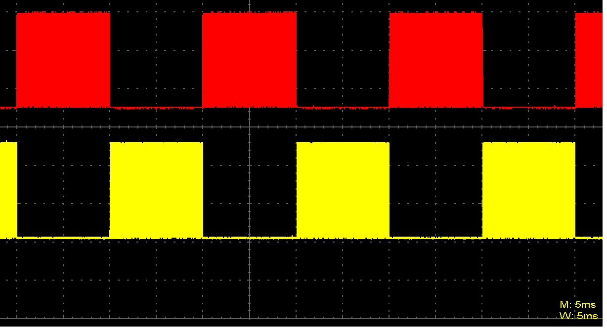
This image from oscilloscope has 5ms/div, so you can see that each signal has a 10ms period.
Another thing we can see here is time between switching pins.For that we reduce at 10us/div and the result is below:
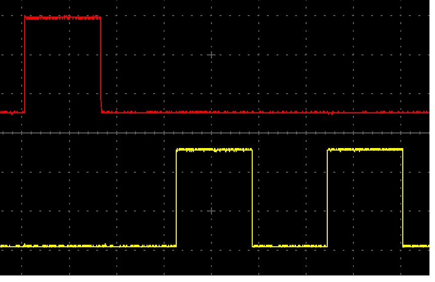

In the image below is represented the output signal from the two pins: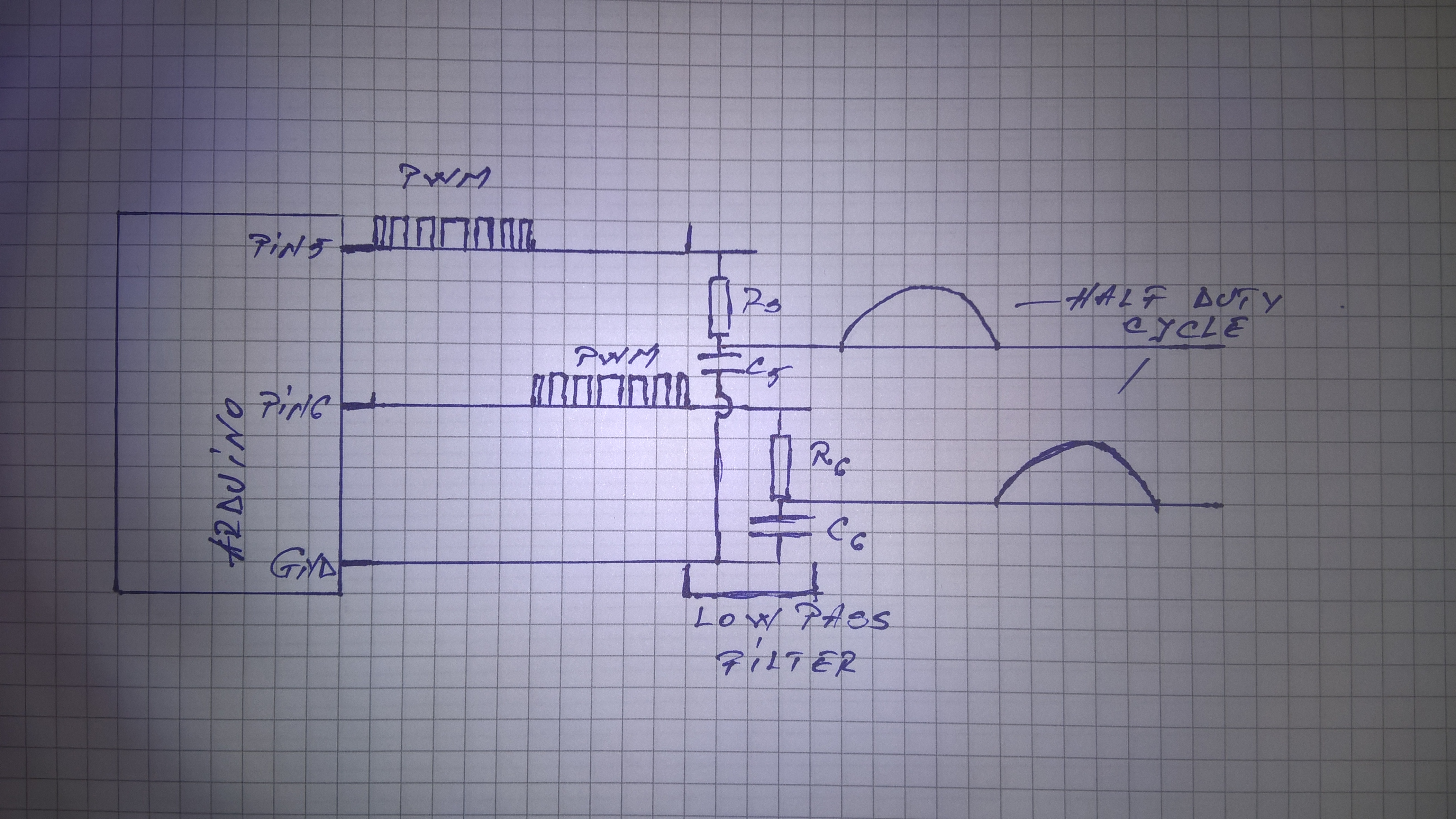

As you can see the output signal is a pwm signal with variable duty cycle and after the low pass filter(R=47ohms and C=22uF) appear a half sinus form.
To have a full sine wave you need to use a H bridge and command it with these two signals (before filter).
Because we visualise the signal on an oscilloscope we have the posibility to make math operation on signal so, if we apply a “minus operation”
we obtain a full sinus wave like from a H bridge.
The program below use a variable duty cycle:
int i=0;
int x=0;
int OK=0;
int sinPWM[]={1,2,5,7,10,12,15,17,19,22,24,27,30,32,34,37,39,42,
44,47,49,52,54,57,59,61,64,66,69,71,73,76,78,80,83,85,88,90,92,94,97,99,
101,103,106,108,110,113,115,117,119,121,124,126,128,130,132,134,136,138,140,142,144,146,
148,150,152,154,156,158,160,162,164,166,168,169,171,173,175,177,178,180,182,184,185,187,188,190,192,193,
195,196,198,199,201,202,204,205,207,208,209,211,212,213,215,216,217,219,220,221,222,223,224,225,226,227,
228,229,230,231,232,233,234,235,236,237,237,238,239,240,240,241,242,242,243,243,244,244,245,245,246,246,
247,247,247,248,248,248,248,249,249,249,249,249,255,255,255,255,249,249,249,249,249,248,
248,248,248,247,247,247,246,246,245,245,244,244,243,243,242,242,241,240,240,239,238,237,237,236,235,234,
233,232,231,230,229,228,227,226,225,224,223,222,221,220,219,217,216,215,213,212,211,209,208,207,205,204,
202,201,199,198,196,195,193,192,190,188,187,185,184,182,180,178,177,175,173,171,169,168,166,164,162,160,
158,156,154,152,150,148,146,144,142,140,138,136,134,132,130,128,126,124,121,119,117,115,113,110,108,106,
103,101,99,97,94,92,90,88,85,83,80,78,76,73,71,69,66,64,61,59,57,54,52,49,47,44,42,39,37,34,32,30,
27,24,22,19,17,15,12,10,7,5,2,1};
void setup() {
Serial.begin(9600);
Serial.begin(9600);
pinMode(5, OUTPUT);
pinMode(6,OUTPUT);
pinMode(6,OUTPUT);
cli();// stop interrupts
TCCR0A=0;//reset the value
TCCR0B=0;//reset the value
TCNT0=0;//reset the value
//0b allow me to write bits in binary
TCCR0A=0b10100001;//phase correct pwm mode
TCCR0B=0b00000001; //no prescaler
TCCR1A=0;//reset the value
TCCR1B=0;//reset the value
TCNT1=0;//reset the value
OCR1A=509;// compare match value
TCCR1B=0b00001001; //WGM12 bit is 1 and no prescaler
TCCR0A=0;//reset the value
TCCR0B=0;//reset the value
TCNT0=0;//reset the value
//0b allow me to write bits in binary
TCCR0A=0b10100001;//phase correct pwm mode
TCCR0B=0b00000001; //no prescaler
TCCR1A=0;//reset the value
TCCR1B=0;//reset the value
TCNT1=0;//reset the value
OCR1A=509;// compare match value
TCCR1B=0b00001001; //WGM12 bit is 1 and no prescaler
TIMSK1 |=(1 << OCIE1A);// enable interrupts
sei();//stop interrupts
}
ISR(TIMER1_COMPA_vect){// interrupt when timer 1 match with OCR1A value
if(i>313 && OK==0){// final value from vector for pin 6
i=0;// go to first value of vector
OK=1;//enable pin 5
}
if(i>313 && OK==1){// final value from vector for pin 5
i=0;//go to firs value of vector
OK=0;//enable pin 6
}
x=sinPWM[i];// x take the value from vector corresponding to position i(i is zero indexed)
i=i+1;// go to the next position
if(OK==0){
OCR0B=0;//make pin 5 0
OCR0A=x;//enable pin 6 to corresponding duty cycle
}
if(OK==1){
OCR0A=0;//make pin 6 0
OCR0B=x;//enable pin 5 to corresponding duty cycle
}
}
void loop() {
}
Now the results before the low pass filter are:

In the image above the red signal is from pin 5 , yellow signal is from pin 6 and the green one is the “minus operation” between the other two.
Now, if we put the oscilloscope probes after filter we have:
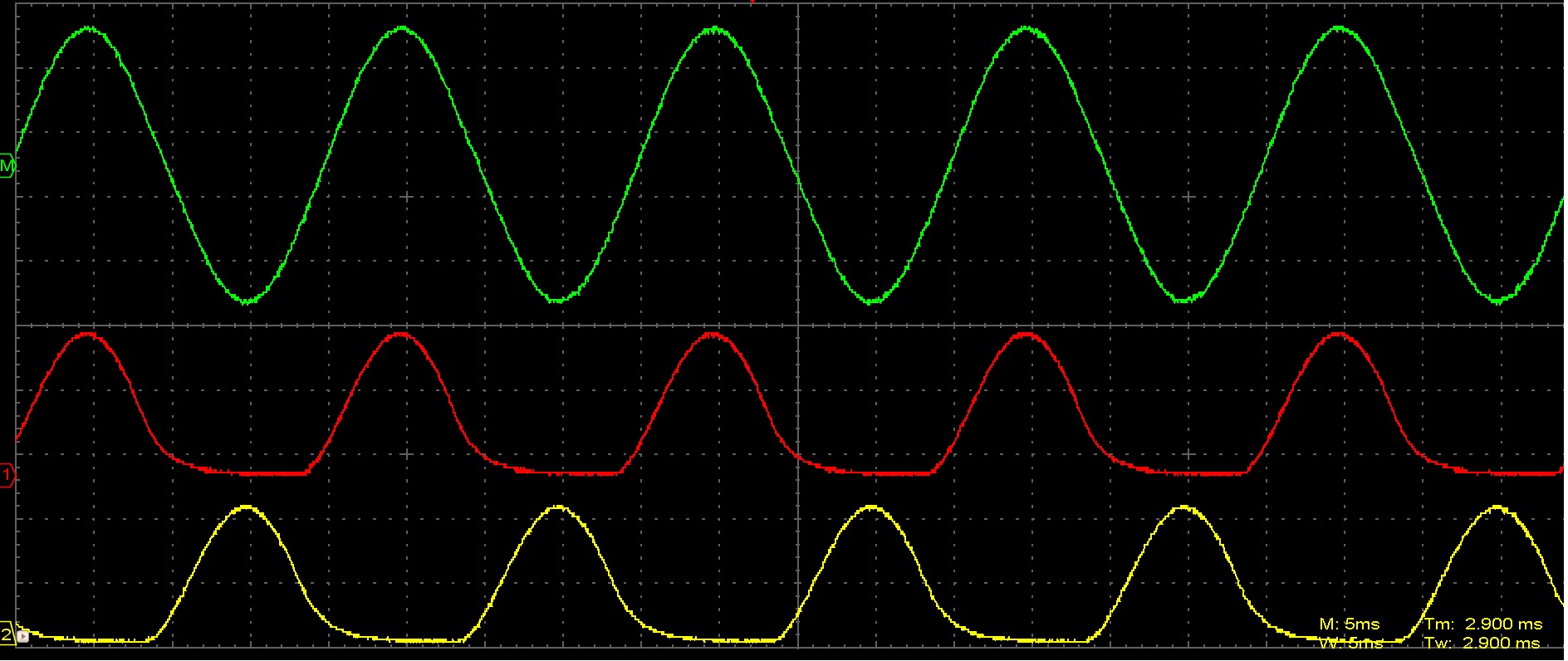
Again, with the program above(with a variable duty cycle) and a mathematichal function we have obtain the signal above but with a H bridge you can obtain a pure sine wave and you can use it in pure sine inverters.
At last the frequency on this application is between 49.94 and 50.02 Hz, in the image below is only on channel 1 because the software of the oscilloscope can’t display the frequency of the “math signal”.

To make an update to this post next is a 60Hz signal.
Before the main program below is the program to generate values for duty cycle(with some differences from the first-it will generate all the values from zero to zero).
The program is:
float x=0;
float y=0;
const float pi=3.14;
int z=0;
float v=0;
int w=0;
boolean OK=true;
void setup() {
Serial.begin(9600);
}
// the loop function runs over and over again forever
void loop() {
if (w==0){
v=x*pi/180; // making deg in radians
y=sin(v); //calculate sinus
z=y*250; // calculate duty cycle(250 not 255 because will help to turn off transistors)
delay(100);
if(OK==true){
x=x+0.689;// increase the angle
}
}
if (x>90){
OK=false;
}
if (OK==false){
x=x-0.689; //decreasing the angle for the other half
}
Serial.println(z);// on the serial monitor will appear duty cycles between 0 and 180 deg
}
Now the main program will consist 260 elements because at last we have the transition between pins, and on the oscilloscope we have a better frequency.
The main program is:
int i=0;
int x=0;
int OK=0;
int sinPWM[]={1,3,6,9,12,15,18,21,24,26,29,32,35,38,41,44,47,50,53,56,59,62,65,68,71,73,76,79,82,85,88,91,93,96,
99,102,104,107,110,112,115,118,120,123,126,128,131,133,136,138,141,143,146,148,151,153,155,158,160,
162,165,167,169,171,173,176,178,180,182,184,186,188,190,192,194,196,197,199,201,203,205,206,208,210,
211,213,214,216,217,219,220,222,223,224,226,227,228,229,230,232,233,234,235,236,237,238,239,239,240,
241,242,243,243,244,244,245,246,246,247,247,247,248,248,248,249,249,249,249,249,249,249,249,249,249,
249,249,248,248,248,247,247,247,246,246,245,244,244,243,243,242,241,240,239,239,238,237,236,235,234,233,
232,230,229,228,227,226,224,223,222,220,219,217,216,214,213,211,210,208,206,205,203,201,199,197,196,194,
192,190,188,186,184,182,180,178,176,173,171,169,167,165,162,160,158,155,153,151,148,146,143,141,138,136,
133,131,128,126,123,120,118,115,112,110,107,104,102,99,96,93,91,88,85,82,79,76,73,71,68,65,62,59,56,53,50,
47,44,41,38,35,32,29,26,24,21,18,15,12,9,6,3,1};
void setup() {
Serial.begin(9600);
Serial.begin(9600);
pinMode(5, OUTPUT);
pinMode(6,OUTPUT);
pinMode(6,OUTPUT);
cli();// stop interrupts
TCCR0A=0;//reset the value
TCCR0B=0;//reset the value
TCNT0=0;//reset the value
//0b allow me to write bits in binary
TCCR0A=0b10100001;//phase correct pwm mode
TCCR0B=0b00000001; //no prescaler
TCCR1A=0;//reset the value
TCCR1B=0;//reset the value
TCNT1=0;//reset the value
OCR1A=509;// compare match value
TCCR1B=0b00001001; //WGM12 bit is 1 and no prescaler
TCCR0A=0;//reset the value
TCCR0B=0;//reset the value
TCNT0=0;//reset the value
//0b allow me to write bits in binary
TCCR0A=0b10100001;//phase correct pwm mode
TCCR0B=0b00000001; //no prescaler
TCCR1A=0;//reset the value
TCCR1B=0;//reset the value
TCNT1=0;//reset the value
OCR1A=509;// compare match value
TCCR1B=0b00001001; //WGM12 bit is 1 and no prescaler
TIMSK1 |=(1 << OCIE1A);// enable interrupts
sei();//stop interrupts
}
ISR(TIMER1_COMPA_vect){// interrupt when timer 1 match with OCR1A value
if(i>260 && OK==0){// final value from vector for pin 6
i=0;// go to first value of vector
OK=1;//enable pin 5
}
if(i>260 && OK==1){// final value from vector for pin 5
i=0;//go to firs value of vector
OK=0;//enable pin 6
}
x=sinPWM[i];// x take the value from vector corresponding to position i(i is zero indexed)
i=i+1;// go to the next position
if(OK==0){
OCR0B=0;//make pin 5 0
OCR0A=x;//enable pin 6 to corresponding duty cycle
}
if(OK==1){
OCR0A=0;//make pin 6 0
OCR0B=x;//enable pin 5 to corresponding duty cycle
}
}
void loop() {
}
The results as pwm signals are:
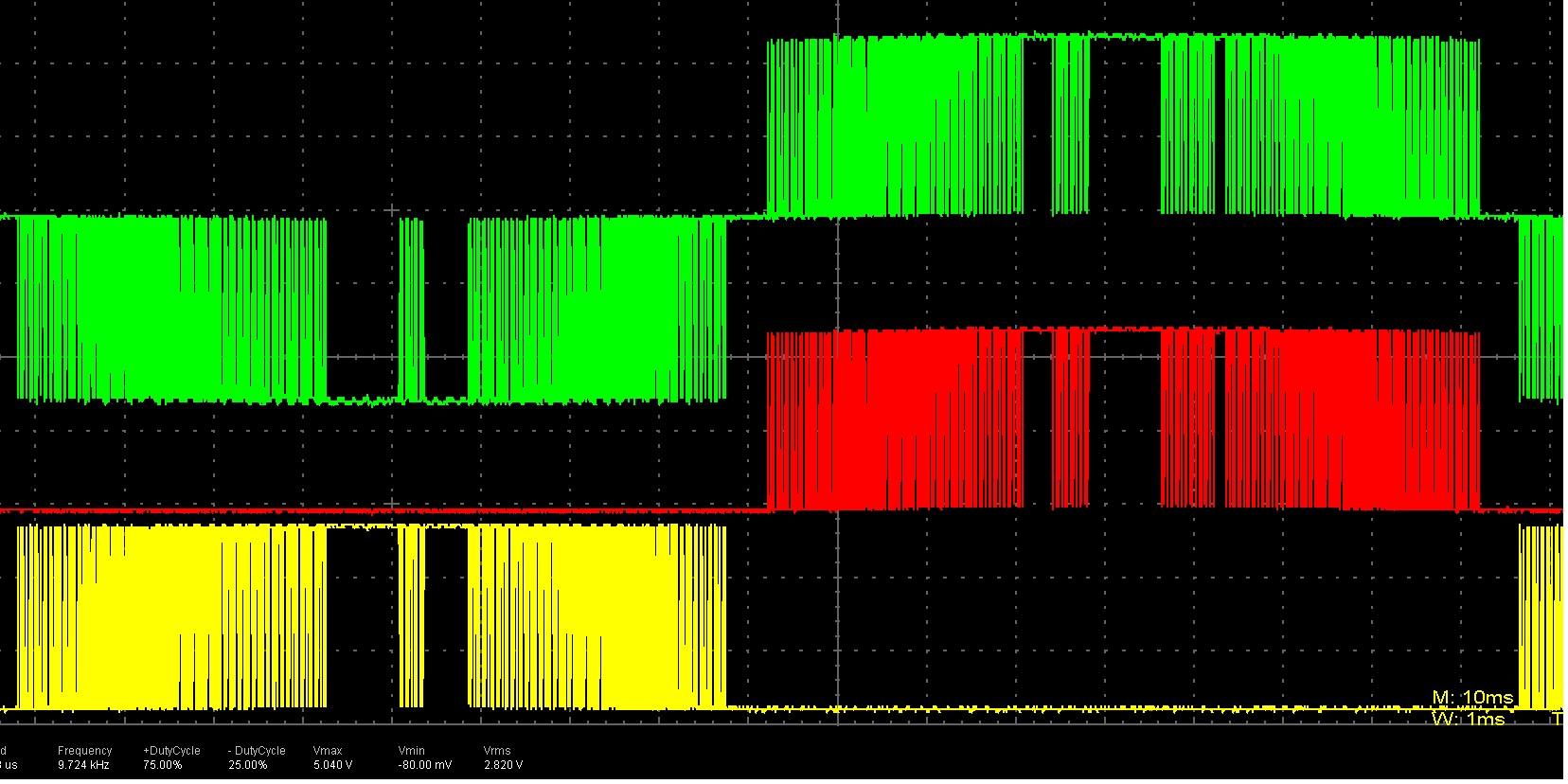
The green signals are the others two combined.
A half sine wave:

In this picture is presented only a half cycle because i have used only one low pass filter(i had only one capacitor) and you can see that the resulting frequency is 60.02 Hz.
The result are better than in the previous example because i have used film capacitor(1uF) and not electrolitic for the low pass filter ( R=220 ohms).
A short video:
Now N=8.3ms/31.8us=261pulses, so the only thing you need to change is the number of pulses and the duty cycle of them. In the vector you should have 261 elements(with different values from the our example) and in the ISR where appear 313 you must have 261(or 260 if give you an more precise frequency).
float sinPWM[]={1,2,5,….1,2,5}
Try to understand all the aspects of the project.
If you want a good article for topology with mosfets here is something that look good(i haven’t build a h bridge for now so i can’t confirm the schematic)
h bridge with mosfets
Again i have no responsability if something go wrong!!!
When you finish the project maybe you’ll share the experience and the results.
Be aware that for transistors you should use the pwm signal not filtered!
https://blogger.googleusercontent.com/img/b/R29vZ2xl/AVvXsEh_yGFRv0VY6Q2I0MhiDjxt_HBMqPWN8Wwx6ektEczjnBqoq6bygnc0PwKI4ZIDyAs-lQAK1JCyxGGEJ2KbJ4grOe5jI62qLL9TF_rMbn5bHL-AGXvBVcw7hTMOEunb_xv7_glCW_JfDlyj/s1600/IR2110+-+7.png
Thanks